
We use traditional nanofabrication techniques and we also develop new nanoscale device fabrication and characterization techniques, in particular those based on electron-beam lithography (EBL) and transmission electron microscopy (TEM).
Read more about some of our prepared nanoscale structures.
Nanogaps
Nanogaps down to sub-nm widths are fabricated on silicon nitride membrane windows using standard electron beam lithography. This is possible because electron backscattering is sufficiently minimized on these substrates to allow for fabrication with nm-scale resolution.
(for more details see also Nanoelectronics-Section)
These nanogaps are compatible with high-resolution transmission electron microscopy. The following image is a micrograph of a 4 nm-large nanogap showing lattice orientation in gold electodes. The grey background shows structure of the silicon nitride substrate.

For more details on the preparation of nanogaps and their use for the measurement of few PbSe nanocrystals:
Michael D. Fischbein and Marija Drndic
“Nanogaps by direct lithography for high-resolution imaging and electronic characterization of nanostructures”
Applied Physics Letters 88 (6), 063116, 2006.
cond-mat/0512128
Transmission Electron Beam Ablation Lithography (TEBAL)
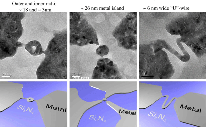
We used a high-resolution transmission electron microscope (TEM) to fabricate metal nanostructures and devices on insulating, silicon nitride (Si3N4) membranes by nanosculpting metal films. Using this top-down, resist-free approach, we have hand-made a wide range of metal nanostructures with sub-nm resolution including nanogaps, nanodiscs, nanorings, nanochannels, nanowires with tailored curvatures and multi-terminal nanogap devices with nanoislands or nanoholes between the terminals. We call this method TEBAL (for transmission electron beam ablation lithography). During TEBAL, the user is able to watch on the fluorescent imaging screen of the TEM the ablation of the unwanted metal, followed by the crystallization of the surrounding metal and the formation of desired geometries. The high resolution, geometrical flexibility and yield make this fabrication method unique and attractive for many applications including nanoelectronics, nanofluidics, plasmonics, nanoparticle/atom manipulation on a chip. Particularly exciting and unique are the nanogap-nanohole devices as they open new opportunities for DNA nanopore sequencing.
If you are interested in any aspect of this method, please contact us with questions or comments.

Arbitrary two-dimensional metal nanostructures and devices connected to larger metal leads are made by nanosculpting thin metal films of silver, gold, aluminum and other metals to form a range of geometries from nanorings to nanowires with tailored curvatures and down to sub-nm dimensions.
The next figure shows three examples of metal nanostructures made by TEBAL on silicon nitride (Si3N4) membranes: a curved, U-shaped nanowire (radius of curvature < 1 nm at the three bends), an eight(8)-terminal nanogap field-effect transistor (FET) geometry for electrical probing along many directions, and a nanoring connected to larger metal leads without contact resistance.
For more details on TEBAL:
Michael D. Fischbein and Marija Drndic
“Sub-10 nm Device Fabrication in a Transmission Electron Microscope”
Nano Letters 7 (5), 1329-1337, 2007.
cond-mat/0611032
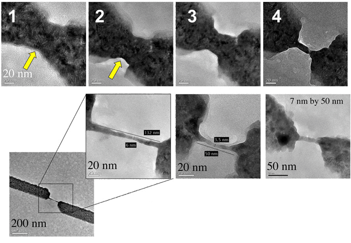
Nanowires
TEBAL can also been used to prepare nanowires.
The following images show several stages of fabrication of nickel and chromium nanowires.
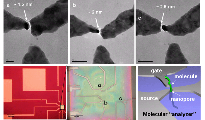
Nanogap-nanohole Field-Effect-Transistors
Nanogap-nanohole (or nanopore) field-effect transistors consist of three electrodes near a nm-size hole in silicon nitride. Images below show nanogaps from 1.5 nm to 2.5 nm made on a single chip where a nanohole spans the gap between two electrodes. The third electrode can be used as a gate electrode. Such devices combine nanopores and nanogaps and are promising new tools for molecular detection and analysis including DNA translocation studies. In these studies molecules translocate in the direction perpendicular to the silicon nitride membrane surface below.
For more details on the preparation of nanohole FETs with TEBAL:
Michael D. Fischbein and Marija Drndic
“Sub-10 nm Device Fabrication in a Transmission Electron Microscope”
Nano Letters 7 (5), 1329-1337, 2007.
cond-mat/0611032